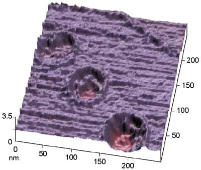
STM image of conducting LB film of
C18H37BEDTTTF (three monolayers) after
local exposure to three electric pulses (duration t=15mcs, voltage U=5V, tip-surface separation S=1nm). Crater-like defects of one monolayer depth are readily seen. LB film was formed by MDT-LB5.
V.A.Bykov. Langmuir-Blodgett films and nanotechnology. Biosensor & Bioelectronics Vol. 11, No. 9, pp.
923-932, 1996