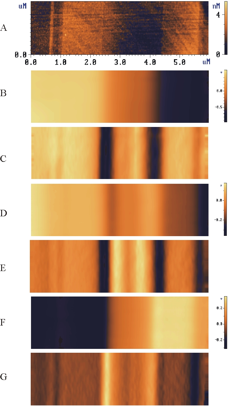
AFM, KPM and Voltage Drop (dV/dx) images of GaAlAs/GaAs
n-i-p laser diode at different applied voltage.
A - AFM topography image. The emitter and waveguide regions are well-observed.
B,C - SKPM and Voltage Drop images at -1.5V (reverse) bias voltage applied.
D,E - SKPM and Voltage Drop images without bias voltage.
F,G - SKPM and Voltage Drop images at +1.5V (forward) bias voltage applied.
Sample of laser diode cleave and images courtesy of Alexander Ankudinov
(group of A.Titkov),
Ioffe Physico-Technical Institute, St. Petersburg, Russia